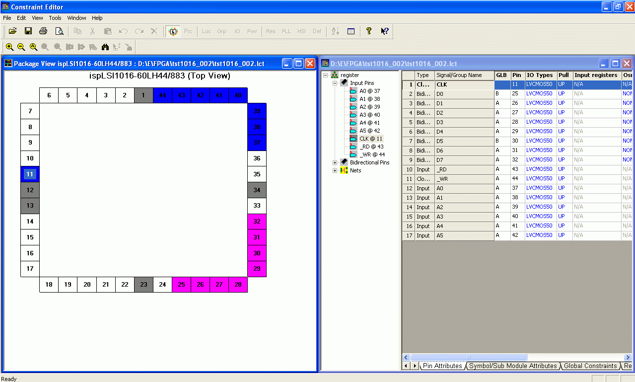
ispLSI1016 interface
A question, a problem or a suggestion, don't hesitate : a little email
ispLSI1016 interface
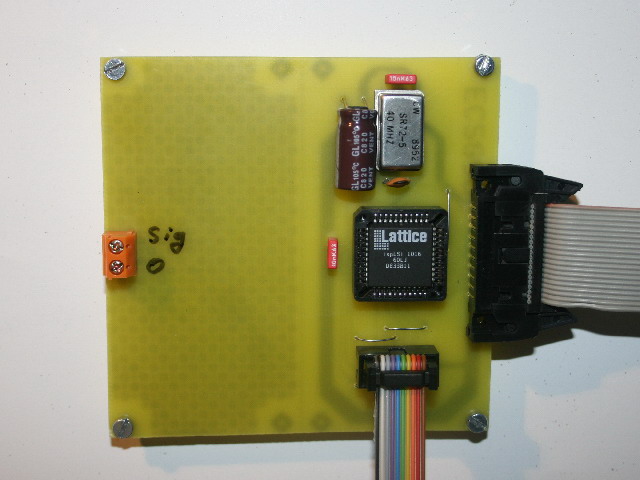
Board which realizes the interface between a Peri1 bus and an ispLSI1016 FPGA from Lattice.
The board also includes an oscilator for the clock of the ispLSI and a large breadboard zone.
Schematic
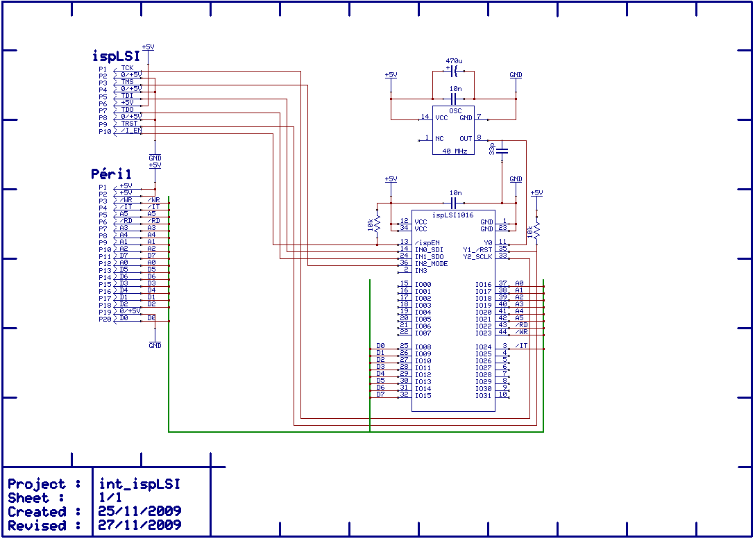
Just 2 components :
- The ispLSI1016,
- An oscilator as an optionnal clock for the ispLSI.
And 2 connectors, one for the Peri1 bus and the other for programming the ispLSI.
PCB
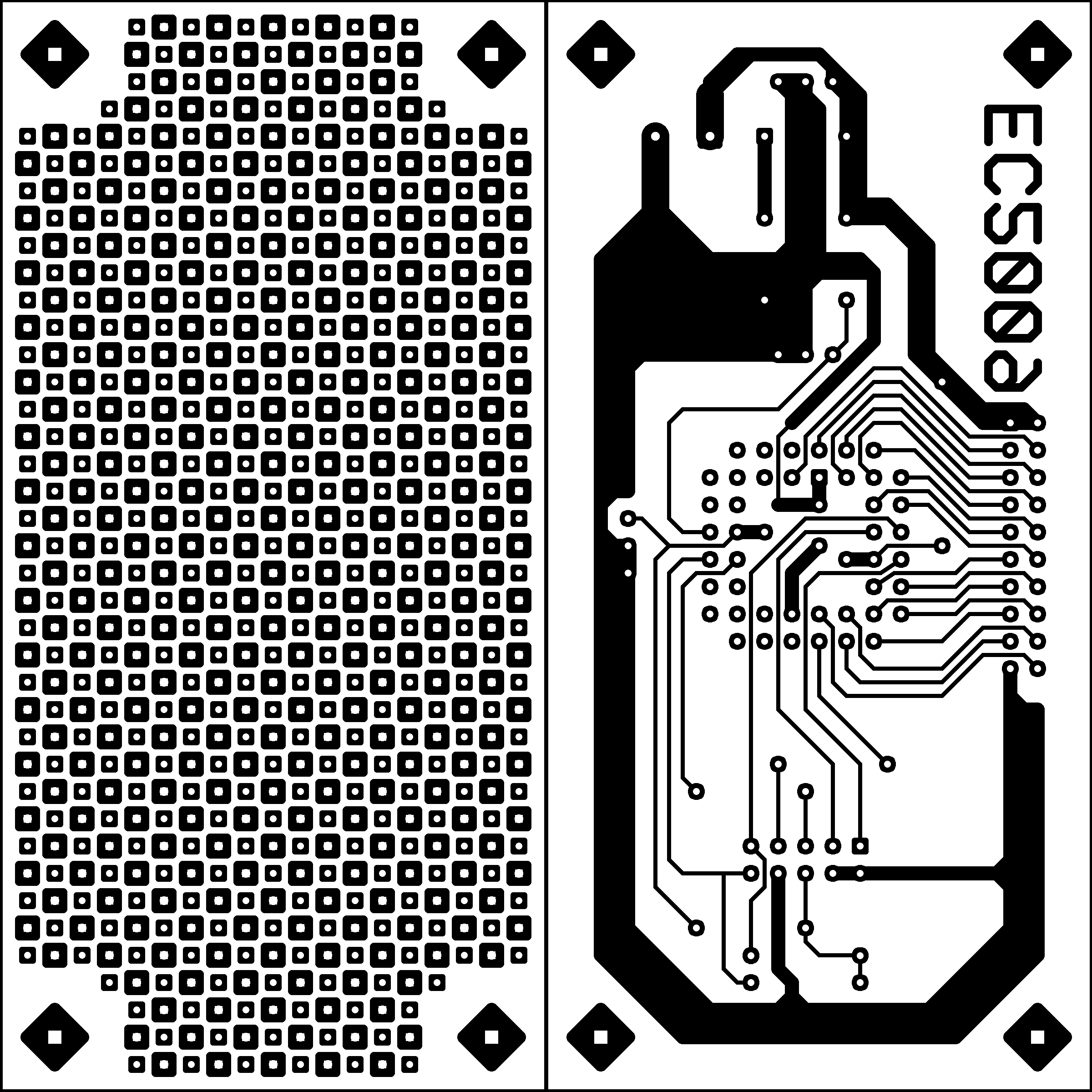
The PCB of the board. All the left side is an optionnal breadboard zone.
Click on the picture to display the full resolution PCB (156 ko).
It is a 4 by 4 inches board (102 by 102 mm) at 600 dpi resolution (when including the breadboard zone).
Component side
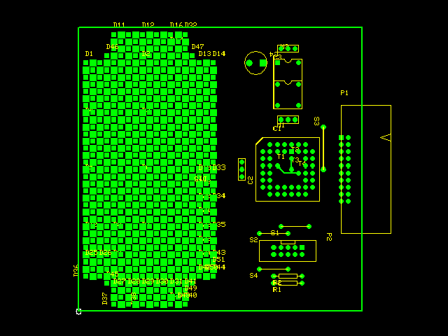
The place of the different components of the board.
6 straps to avoid a double sided board, 2 of which under the ispLSI1016.
ispLSI firmware
You will find here (18 ko) the ispLSI part of a test sofware checking that the main inputs/outputs are OK.
Test program
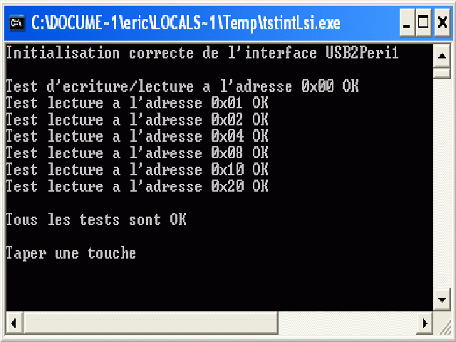
You will find here (22 ko) the PC part of a test software using the USB2Peri1 interface.
If all is OK, you should read something like this screen or an error diagnostic.