PCB manufacture
A question, a problem or a suggestion, don't hesitate : a little email
Step by step, the manufacture of an home made printed circuit board (PCB).
This web page describes the process I use the more frequently but many variants exist :
- For double sided circuits,
- Using specific papers for specific PCB printing tools (transparencies,...).
With care, you can print 3 or 4 traces for a tenth of inch.
Minimum tools
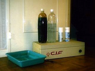
- A tub to develop the film and to engrave,
- A film flasher (or a specific bulb),
- PCB developer liquid,
- PCB engraver liquid,
- Specific spray to make transparent the trace of the circuit.
Cut the circuit
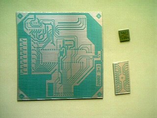
First step : cut the circuit with specific dimensions in a (positive) sensitive copper board (simple or double sided).
I always use some small sample to check the flashing time especially when I change my sensitive copper board supplier.
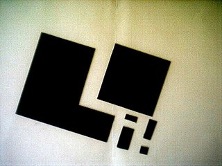
Print the artwork
Next step : realize a trace of the circuit. I use a laser printer with a 600 dpi resolution.
The trace must be bottom printed because the printed face is place against the circuit (nevertheless a black line on the trace is a copper trace on the circuit with this "positive" method).
A copy of the circuit can also be used (trim the zoom to reach exact dimensions).
Flash the circuit
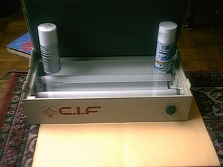
Next step : make the trace of the circuit transparent to the light used by the flasher. I use "Diaphane" spray from KF.
Completely wet the trace and wait until have a dry aspect.
After that, flash the circuit. I use a flash of 4 minutes with a double pipe flasher (don't forget to remove the back film protecting the sensitive layer !).
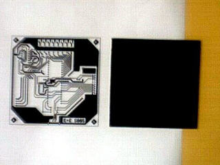
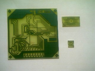
Develop the film
Develop the flashed circuit in the specific developer liquid during about 1 minute (be careful the products are dangerous).
The traces must be sharp and have a good contrast (usually the trace are blue).
Some corrections can be done using specific felt-tip and a cutter.
Engrave the circuit
Use the PCB engraver liquid to remove the copper not protected by the blue film (more than a quarter of hour at ambient temperature).
If you don't use immediately the circuit, let the blue film to avoid any copper oxidation.
To remove the film, the simplest method is to use a acetone drenched cotton (nail varnish remover).
Drill and solder
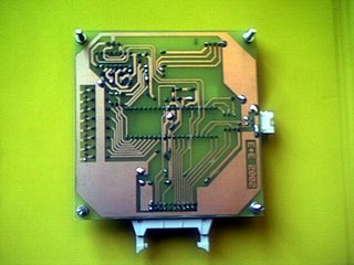
Drill the circuit (0,6 to 0,8 mm drill for current components).
Solder the component and check than the weld are bright.
Remove the solder deoxidize traces (small spots like varnish) using acetone.
Use varnish to protect the copper (after tests !!!).
Optional tools
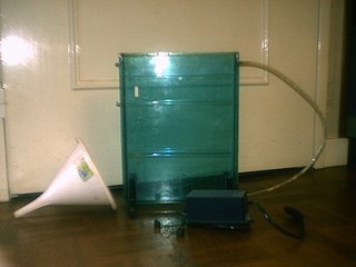
Some tools are useful to make the process quicker and easier :
- An engraver with an aquarium pump and a slightly warmed engraver liquid,
- A vertical mounted driller to be sure to make vertical and parallel holes,
- Funnel, protecting gloves,...